

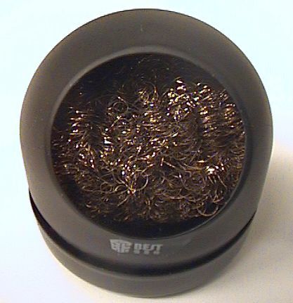
These 2200W wifi controlled Smart Sockets are available from suppliers on Ebay for about £15 - they are available with various Mains input plug formats (Europe, UK, US), they have multi-standard Mains output sockets, onboard USB charging socket, onboard configuration push button, and 2 onboard LEDs (green and blue).
In a Nutshell
This article is more than just a tutorial, it is also a ‘Goodies Bag’ offering some other helpful nuggets. The tutorial shows how to hack the Smart Socket to remove its original wifi board and fit an alternative ESP8266 stripboard DIY replacement, resulting in a user-programmable versatile switched-mains power socket that is capable of being used with any of the ESP8266 programming and control alternatives such as AT commands, Lua scripts, MicroPython, Arduino sketches etc, and particularly Souliss (link to go here).
It is a safe low voltage hack because none of the potentially dangerous Mains stuff is involved, and the hack can be powered via a 5v USB cable for testing and flashing, so the Smart Socket is only plugged into the Mains for usage after being completed.
It uses an ESP-12 or similar (ESP-202, ESP-07 etc), a BMP180 temp+humidity sensor (or BME280 which also includes barometric pressure), a small logic level converter module, four 10K resistors, and a 0.1uF bypass capacitor.
Note: If you would prefer to include this hack functionality into your own home-built switched socket(s), see the Footnotes section at the end.
The Souliss example sketch can integrate the Smart Socket as a peer node or gateway on the Souliss automation network (the gateway can also include peer functionality) thereby allowing it to be controlled by android devices using SoulissApp.
###Why Bother?
If you are a visitor to Souliss and wondering why bother going to the effort of ESP-8266 conversion just to arrive back at a similar starting point with phone app control of the Smart Socket, here’s a brief overview of Souliss to explain why…
Compare Souliss to the global postal service:
- Souliss peer ‘nodes’ are the equivalent of postal addresses.
- The Souliss ‘gateway’ is the local post office which routes all unopened mail from the sending addresses to the appropriate delivery addresses.
- Postal address ‘nodes’ may have multiple mail-box ‘slots’ for multiple residents (GPIO slots).
Sure, you could create an alternative local delivery system, but the real power of the postal service lies in its ability to reliably deliver messages globally from door to door anywhere around the world without the end-users ever needing to know details of the road, rail, sea and air transport stages that were required for the delivery. Similarly, the true power of Souliss lies in its sophisticated hidden delivery infrastructure which allows messages to be automatically routed and transparently bridged across different types of network media (Ethernet, Wifi, RF, RS485, Serial etc). Souliss also includes a ‘quickie’ postcard-like system for optimal communication efficiency which allows nodes to send concise ‘typical’ standardised event-related messages which can be automatically responded to by receiving nodes where applicable, and the free android SoulissApp contains appropriate corresponding controls and status displays for these standardised ‘typical’ messages (plus other goodies such as voice control). Peer to peer interaction is autonomous, so no additional controlling hardware or software is required, but Souliss can be integrated with OpenHAB (open-source) home automation computer systems if wished. It is also possible to access nodes via web browsers. Software will soon be available that can treat a Souliss ESP node plus its relevent sensors and devices as a simple ‘black box’ that can easily be configured via web page then re-programmed wirelessly ‘Over The Air’ without requiring any programming skills or knowledge… essentially ‘Souliss IOT for Dummies’ like me.
What all this means is that with minimal effort and programming knowledge it is relatively easy to get Souliss nodes interacting with each other across different network media, and to have overall android or web remote control and monitoring of everything, on an extensible automation framework which can accomodate evolving automation systems without requiring any major restructuring, and because Souliss runs on the ubiquitous Arduino framework its nodes can offer integration of almost anything that can be done using an Arduino or ESP8266.
And all for free, because Souliss is open-source, and driven by a knowledgable and welcoming community who are ever reaching out to new horizons, and ever ready to give help and advice whenever needed.
So that is the incentive for using Souliss, but it is not an essential requirement of this hardware hack, which allows the ESP8266 to be used with whatever software is preferred.
###Smart Socket Hack
This hack is intended for DIY construction on a postage stamp sized piece of stripboard, and is aimed at people like myself who don’t have any PCB design or manufacturing resources.
The hack has a basic Souliss sketch available to provide quick and simple Android remote control of the Smart Socket, but the real benefit comes from what else is possible.
For example, the switched-socket hack also includes an internal temp+humidity sensor which offers potential for environmental monitoring using SoulissApp or Internet Web Browser, plus automatic environmental triggering of other peer to peer nodes, and even the potential for the Smart Socket to be a local self-contained programmable thermostat.
Additionally, other external sensors can be plugged in via the USB socket - perhaps a PIR sensor for occupancy detection, or an LDR for automatic light level switching, or both together, plus almost any other analog and digital sensors you could realistically need.
The USB socket also provides easy external ‘flashing’ access to the ESP using ‘mode-sharing’.
All the ESP hack hardware details are offered, but it is for users to provide appropriate software to exploit their hardware potential.
###Onboard Facilities
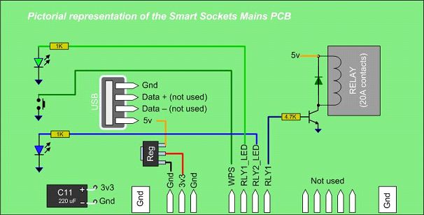
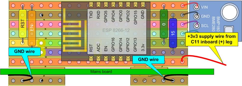
The interesting elements of the Smart Socket are a 3.3v regulator, two LEDs, a pushbutton, a USB charging socket, and a transistor-driven 20A relay with ‘back-emf’ protection diode.
This hack uses a couple of GPIOs to provide an i2c bus for sensors, a couple more for relay and button controls, and optionally a couple for independent control of the 2 LEDS.
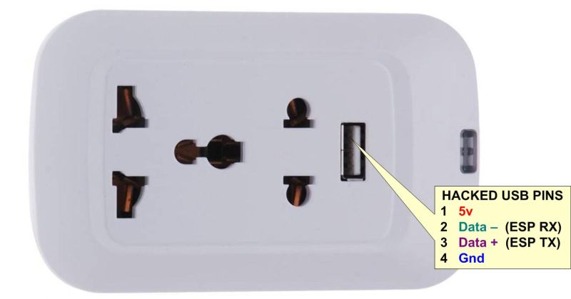
###USB Charging Socket
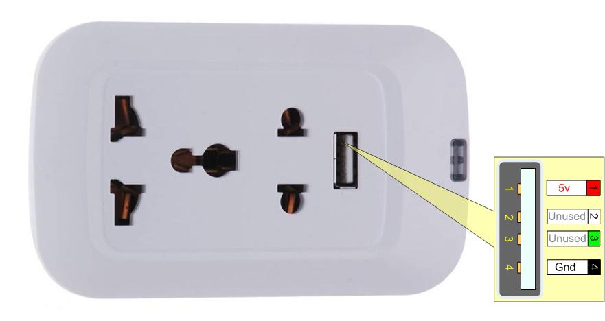
The Smart Socket has a USB charging socket which provides 5v and Gnd on the outer pins.
The USB 5v also supplies a 3.3v regulator on the Mains board which powers the wifi board.
A useful consequence of this is that the onboard electronics and hack can be safely tested or re-flashed simply by plugging in an external 5v USB male cable into the USB socket, without the Smart Socket being connected to the Mains or being Live during testing or re-flashing.
An added bonus is that the 2 inner USB serial data pins which are not being used by the Smart Socket are therefore available for hack purposes, and can provide:
- Quick plug-in external access to RX and TX for easy re-flashing.
- Quick plug-in access of external analog and digital sensors.
- Quick plug-in access for re-flashing AND external sensors - this takes advantage of the fact that when in flashing mode the GPIOs are floating, and when in normal mode the TX and RX lines are floating… so the 2 USB data wires can be ‘mode shared’ without conflict.
###Hack Circuit
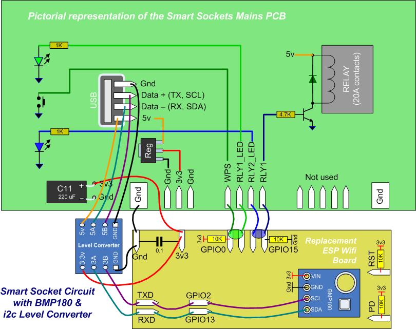
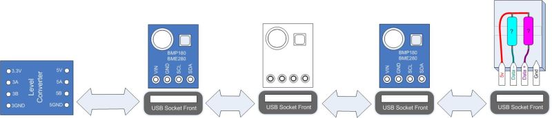
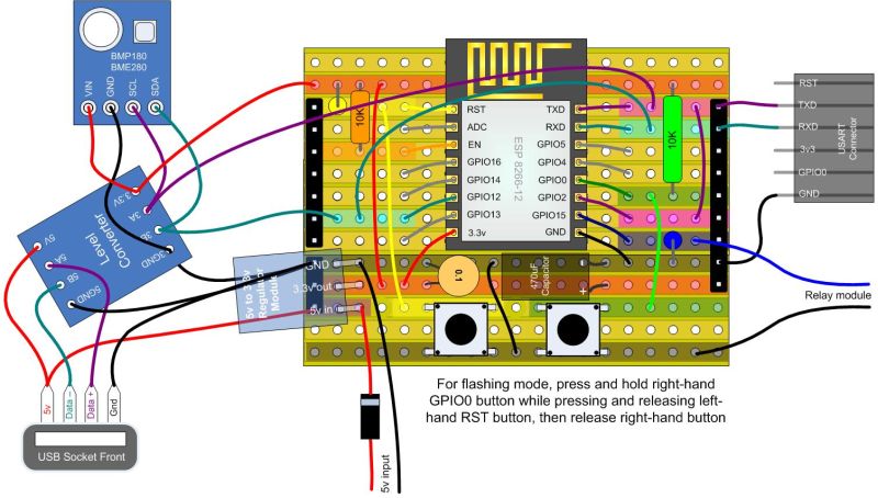
This hack uses i2c to communicate with internal and external sensors, and so uses a Logic level Converter module to interface the ESP 3.3v i2c pins to the 5v USB socket.
GPIO2 is used for SCL because it requires a pullup, and the BMP180 internal sensor already has 4.7K i2c pullups on board, which can conveniently also be used for the GPIO2 pullup.
GPIO13 is used for SDA, with similar i2c pullup from the BMP180.
RX is paired with GPIO13 for mode-sharing of SDA on the USB (-) data line.
TX is paired with GPIO2 for mode-sharing of SCL on the USB (+) data line.
GPIO0 is used for reading the ‘WPS’ button, allowing the button to conveniently set the ESP into flashing mode at Reset/PowerOn, and also be used for user input if required.
GPIO15 is used for the ‘active high’ RLY1 relay because it needs a pulldown resistor anyway.
By default the hack board track bridges the Green RLY1_LED to WPS for visual confirmation of button presses, and similarly bridges the Blue RLY2_LED to RLY1 to echo relay status.
(The relay draws negligable current because of it’s 4.7K transistor base resistor, and the LEDS have 1K series limiting resistors, so each adds less than 5mA load to a GPIOs 12mA max output)
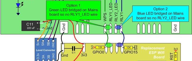
Options 1 & 2 omit the LED wires by bridging the LEDS on the Mains board solder pads.
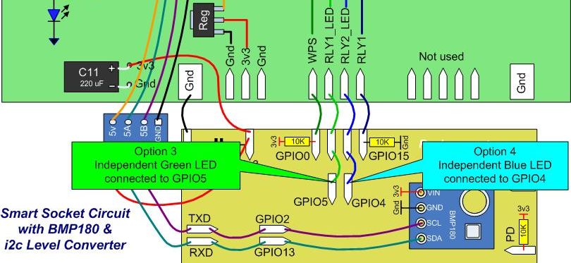
Option 3 uses GPIO5 and a track cut to give independent software control of the Green LED.
Option 4 uses GPIO4 and a track cut to give independent software control of the Blue LED.
Option 5 simply replaces the BMP180 with a BME280 to also read barometric pessure.
That’s quite a lot of functionality to squeeze onto a stripboard area the size of a postage stamp. All the necessary information is present, so If you are confident of where you’re going and how to get there then feel free to go ahead and ‘do your own thing’, but be aware that even with much careful planning there is only just enough room for things to fit, so if you prefer to tread in known footsteps then follow the step-by-step instructions carefully. No electronics knowledge is required, just some competence with a soldering iron and the ability to use a small file and hacksaw blade, but you are assumed to already know how to ‘flash’ your ESP.
Many accompanying pictures and diagrams have been included in an effort to lead by example. Besides showing what to do, they also show what’s already been done and therefore is plainly possible, and should offer confidence that if a short-sighted pensioner (me) can do this hack then anybody else can too. When you are ready, let’s get started.
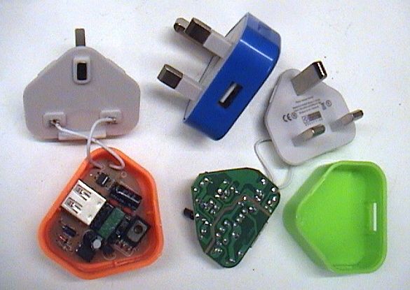
###Disassembly
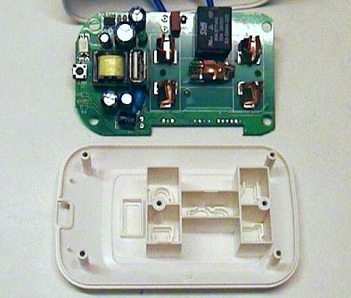
Remove the screws and the front plastic cover, taking careful note of the location and positioning of a loose un-attached clear piece of plastic which is sandwiched underneath the front cover - it’s placement is not particularly obvious, but it is there for a reason (safety), so needs properly replacing again during final re-assembly.
None of the Mains stuff needs to be interfered with, and the hack is easily achieved with the thick blue internal Mains wires still attached, so leave them alone to avoid any problems.
###Connections
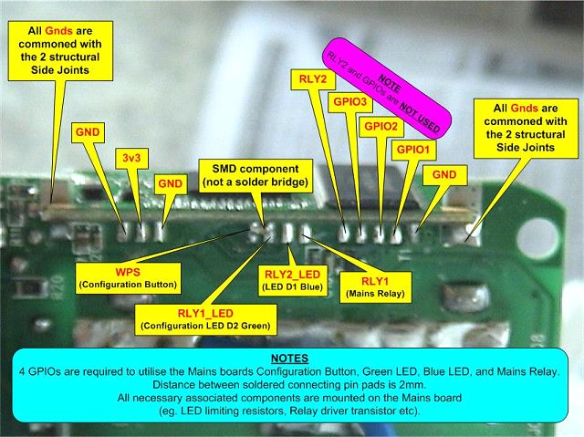
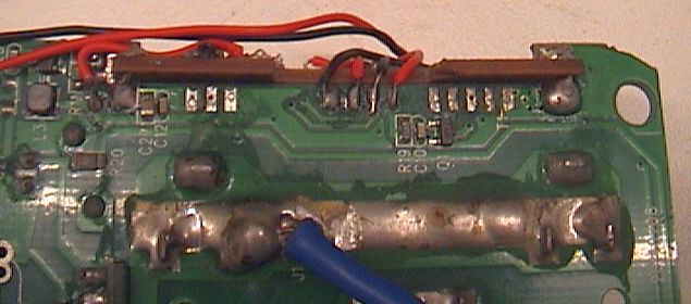
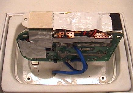
Looking underneath the Mains pcb, and ignoring the 2 larger structural side joints for the moment, you will see three groups of 3, 4, and 5 small solder pads which attach the wifi pcb to the Mains pcb (see the pic above).
From left to right, the first group of 3 are: Gnd, 3v3, Gnd
The second group of 4 are: WPS, RLY1_LED, RLY2_LED, RLY1
- WPS goes to the mains boards ‘config’ push-button which switches directly to Gnd.
- RLY1_LED goes to an ‘active-high’ green LED via a 1K series current limiting resistor.
- RLY2_LED goes to an ‘active-high’ blue LED via a 1K series current limiting resistor.
- RLY1 goes to the 20A Mains switching relay via a transistor and its 4.7K ‘base’ resistor.
- The third group of 5 are just spare outputs from the wifi board and are not used by the Smart Socket, so you don’t need to worry about reconnecting to any of those.
Nor do you need to worry about reconnecting to the 2 Gnd pads each side of the 3v3, because the 2 side structural joints are both Gnds anyway and much easier to solder to, and likewise it is easier to pick up +3.3v from the Mains board C11 capacitor than the smaller 3v3 solderpad.
Also don’t worry about the tiny SMD component which is bridging the WPS pin to its neighbour, because we won’t be needing that anymore.
###Better Than Expected
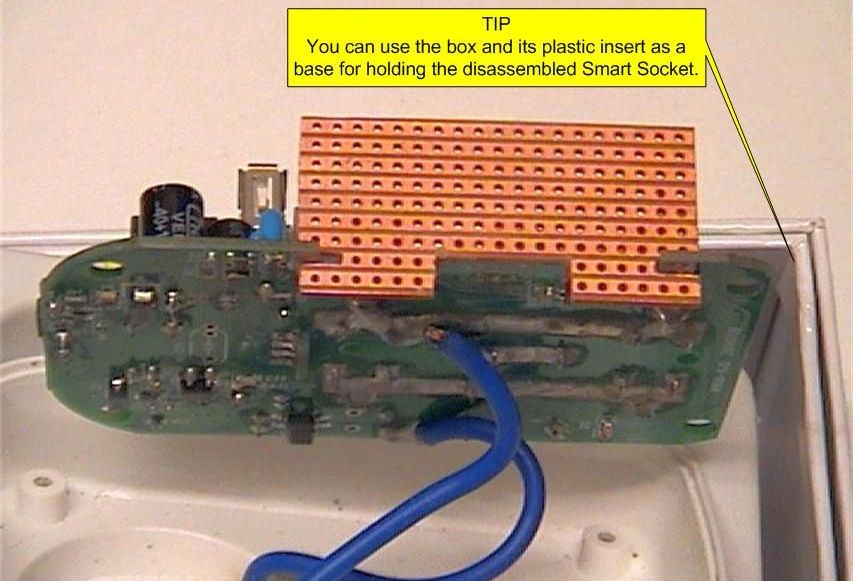
Out of the 12 small pads that need de-soldering to remove the old wifi board, only the centre group of 4 require reconnection again (and perhaps only 2 of them, depending on chosen options). And to make things easier for soldering wires to the 4 solder pads we will be cutting out a lower access slot on the replacement wifi board (see above) to offer better unhindered access… so hopefully the job is not as daunting as it may have initially appeared.
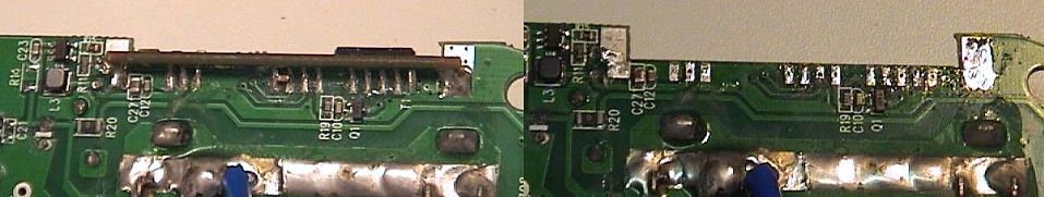
I had been expecting removal problems, but it was much easier than first thought. All the pads and joints de-soldered ok (including the SMD component), and the wifi module was able to be removed in one piece without causing any damage or needing to nibble bits away with cutters. It’s certainly worth de-soldering everything twice though, and using a magnifier to double-check for remaining solder splashes rather than risk ripping off any pads or tracks.
After the original wifi board is removed, re-tin the required group of 4 pads on the Mains board with a blob of solder to aid re-attaching wires. Don’t re-tin the side structural joints yet though, because that could obstruct sliding the replacement board over the slots.
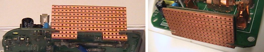
###A Tight Squeeze
If you view the underside of the top cover you can see the integral plastic walls which fit over and around the Mains pins to insulate them from the rest of the protruding electronics.
The position of the insulating walls is marked by white lines on the Mains board pcb, so you can use the line as a guide of how much room is available to fit your hack into - everything on the wifi board needs to fit between the white line and outside edge of the Mains board.
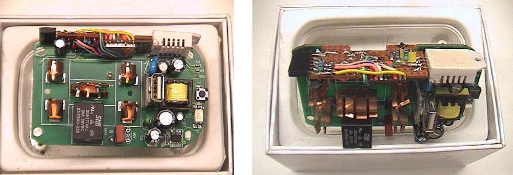
(Pictures of an earlier hack version which included internal DHT sensor and flashing socket)
Follow the instructions carefully and everything fits in ok as shown above - there is not much room to get away with poor soldering though, so the following soldering tips are for those who would welcome them to help improve results, and for others to just skip over.
###Soldering Tips
My own soldering is terrible due to poor eyesight… a case of take aim, dive in for a couple of seconds (timing is everything) then check for damage afterwards with a magnifier (I sometimes miss target completely and discover I’ve soldered an empty adjacent track). So I wouldn’t have a hope in hell of soldering anything if I didn’t heed the following points.
The difference between soldering success or failure is mainly just a matter of having the patience for cleanliness and attention to detail. Impatient or lazy soldering shortcuts inevitably have unwanted consequences… which may seem obvious when you know, but can be a hard lesson to learn, and makes much more sense if you know the reasons why.
Soldering requires heating the local area of the two items to be joined sufficiently for the solder to melt into them and create a molecular bond… so what’s to go wrong?
Well, if heat is applied for too long (for whatever reason, and there are many) it causes overheating of surrounding areas, resulting in charred insulation, naked wires, de-laminated tracks, possibly even component damage. If that sounds familiar, then there is room for improvement, which is fairly easy once you know the reasons for the problems, and how to avoid them.
Solder will only fuse with clean metal, so any impurites will hinder or prevent it from fusing. Therefore ensure no plastic cable insulation can make contact with the joint, or it will contaminate the area and repel the solder away to prevent it from bonding.
Gold is used for contacts because it doesn’t react with air to cause the surface corrosion problems that plague copper and alluminium. Those cheaper conductive metals just have a spray laquer coating to act as an air barrier, because without protection the copper will react with oxygen in the air to form a tarnished green copper oxide coating, and aluminium will similarly go black. But oxides aren’t metal, so they will repel solder. Fine abrasive paper can get back to clean shiny metal suitable for soldering, but it won’t last long.
Multi-core solder contains veins of flux, which acts like a sort of active detergent for breaking down the surface tension barriers between the different metals to help the solder ‘run’ and flow evenly between them. But the active life of hot flux is brief (it’s the few seconds of wispy smoke seen from freshly melted solder), so continued heating just leaves a charred contaminating residue which actually repels solder and prevents it from flowing - and continued stubborn overheating inevitably makes things worse, eventually degrading the conductive metalic solder into a dirty carbonised resistive blob of impurities which will never bond to metal… resulting in a mechanically and electrically unsafe ‘dry joint’.
To avoid that, the hot clean soldering iron tip needs to be applied to the clean joint for maximum heat transfer for minimum time necessary for the solder to run and fuse into the metals - ideally for just a brief ‘dab’ of a second or two. But before even trying, touch solder onto the soldering iron tip to make sure the solder melts quickly (within 1 second) - because the dirtier the tip, the poorer the heat transfer, the longer it takes the solder to melt and flow… and every second of excessive heat on the joint can be causing worsening damage.
Don’t leave the soldering iron switched on when it’s not being used. Don’t leave the heated tip to dry out for any length of time, keep it ‘whetted’ with solder to prevent it burning. The tip should be shiny silver, any dullness shows a coating of impurities building up which will act as a barrier to heat transfer as well as contaminate any fresh solder and flux applied to the joint. So clean the tip frequently on a damp sponge to remove the dead solder, then ‘whet’ it again with a drop of new solder. And do it before every joint… a clean fresh bead of solder on the tip offers much better surface contact area and quicker heat transfer than the small point of contact of a crusty dry tip.
Dirty residues will still gradually build up and blacken the tip anyway, causing contamination of the fresh solder and flux before it can do its job, but a quick poke into a metal mesh tip cleaner then a fresh blob of solder should make the tip shiny again.
All surfaces should be in good physical contact with each other to give good heat transfer, otherwise it is effectively trying to create a hot solder bridge across a colder air gap between surfaces at different temperatures… which ain’t gonna work!
It is important for the soldering iron tip to make good contact with both surfaces to be joined at the same time so that they both heat equally quickly, because if the tip only touches one surface then the heat must transfer all the way through that first item before it can get to the second surface sufficient to fuse solder into the metal… by which time the first surface is already overheating and causing problems.
The flat surface of a bevel or chisel tip provides a bigger surface contact area for increased and quicker heat transfer from the iron. If using a pointed tip, instead of using the pointy end, try using its side, held parallel to the joint to offer more side surface contact area.
The first stage of the hack is to create a stripboard carrier, so there’s no way the copper track will be clean after such handling, Invisible finger-prints are a greasy mask to flux chemistry which repels molten solder and prevents it bonding to the metal below, so it is important to ensure no contaminants are lurking on any surface to act as a barrier which interferes with the flux process and obstructs the clean molecular flow of the solder. I have an old toothbrush and jar of acetone on hand to ensure removal of any invisible sweaty fingerprints, and some fine abrasive paper for making dull surfaces shiny… but things don’t stay shiny for long, so clean just before use.
Due to the tight squeeze, some wires need soldering directly to the copper tracks (rather than the usual luxury of soldering convenient conductors poking through from the component side). So although it might seem convenient to poke a trimmed wire end into a handy hole on the copper side for soldering to the track, the tip will have so little conductor available for heat transfer that it will end up melting the plastic insulation which will contaminate both flux and solder, requiring even more heat, making the mess ever worse.
The solution is easy… pre-solder (‘tin’) the required area of copper track first, and also the bared cable end, then bend it at right-angles and trim off the surplus. Leave sufficient tinned conducter sticking out sideways from the insulation to provide good physical contact with the track and offer somewhere more tangible for ‘dabbing’ the freshly-cleaned and ‘whetted’ tip in order to quickly fuse the two pre-soldered surfaces together. If it takes long enough to burn your fingers while holding the wire in place, then it’s taken too long - and if you jerk away and cause movement in the molten solder just as it’s solidifying it will cause it to crystalise into a dull dry joint that has resistance and can cause all sorts of problems.
The melting point of solder is obviously much lower than of the metals to be soldered, so when in doubt, remember the surest way to ensure a good, quick, clean joint is to pre-solder the two surfaces first. This allows both surfaces to already have a fused layer of solder so that when they are brought together for joining it takes significantly less time heating the two touching pre-soldered surfaces sufficient to re-melt together, than it would to also heat up their underlying metal surfaces sufficient for solder to fuse into the metal.
Lastly, if you don’t want shiny copper tracks and joints to tarnish and corrode, brush them clean with solvent to remove flux residue, then seal from the air with a light spray of laquer.
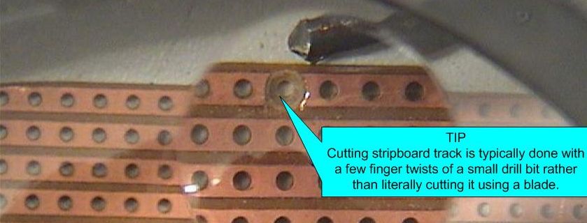
###Stripboard
The key to success for this Smart Socket hack is to pre-prepare a suitable replacement wifi carrier board from some stripboard. It is not difficult, and just needs a bit of care and patience - you need to get this right though, because available space is at a premium, and the hack instructions depend on a replacement carrier board which is the same as shown.
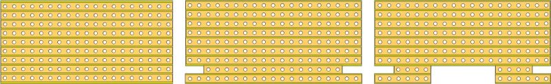
Cut out a 19 holes by 9 holes stripboard blank, then cut out the 2 side ‘locating’ slots (using the original wifi board as a template), then cut out the lower ‘access’ slot as shown above.
Check that it slides onto the Mains board ok (copper side out). Also check it against the original wifi board to ensure it does not stick up higher, or hang lower, and if so, file level.
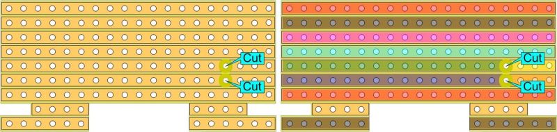
Cut the tracks where shown above, the coloured overlays have been added to help visualise circuit connections and serve as an aid for subsequent component and wiring placement.
###Construction Overview
The BMP180 (or BME280) is connected by short wires to offer some slight flexibility in its positioning. The level converter at the opposite end is connected by longer wires to allow it to be hinged around and folded back tight against the outboard copper side of the ESP board, preferably into the unsoldered track area behind the ESP so it can fit more flush. The replacement wifi board needs to slot over the Mains board component side first (inboard), therefore nothing can be mounted on the component side in the area between the two side slots which could prevent the board from being fully located. This means that the GND link wire (black) and 0.1uF bypass capacitor both need soldering onto the outboard side directly to the copper tracks. Similarly for the solder pad ‘flying’ wires routed from underneath the Mains board. All these outboard items can be soldered to anywhere along their respective tracks - their locations on the diagram are shown for clarity, not best fit, so try to keep them clear of the area where you wish the level converter to be ‘hinged’ into.
###Construction Details
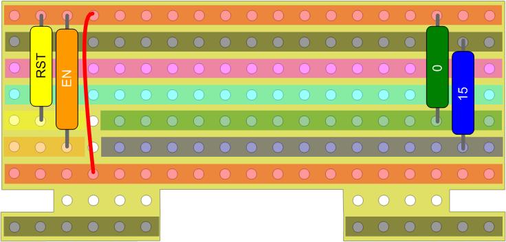
Solder the component-side jumper wire to link up the two +3.3v (red) rails as shown above. Install the 4 resistors. Values aren’t critical, you can use anything from a couple of K up to 20K, but for RST and EN you may want to tend towards lower values for better stability.
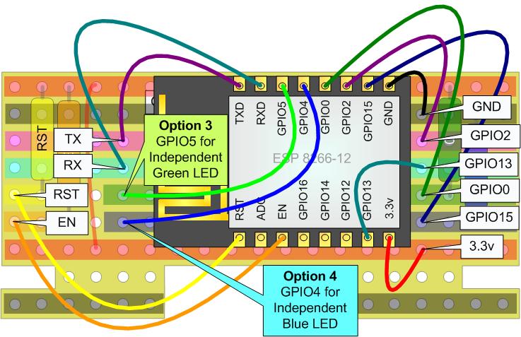
Solder wires to the ESP - including the 2 option wires if required - and ‘stick’ the ESP to the board with some double-sided tape, then connect it up as shown above. The long looping wires are only shown for diagram clarity, but in practice they need to be routed neatly and as short as practical, and cannot stick out above the top or below the bottom of the ESP.
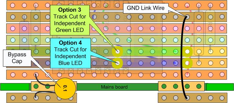
Install the 0.1uF Bypass Cap and GND Link Wire directly on to the copper track side. If requiring Option 3 or 4 for Independent LEDs, make the appropriate track cuts.
Connect the sensor with sufficient ‘slack’ to allow some flexibility for best positioning.
Connect the Level Converter with wires of sufficient length to allow the module to be hinged around and laid flat to the un-used copper area behind the ESP (see below). Don’t connect the USB ‘flying’ wires yet because they are only shown above for circuit clarification.
Check that the board stills fits onto the Mains board ok, then remove it again.
###Board Installation
Solder a +3v3 connecting wire to the inboard (+) leg of capacitor C11 on the Mains board.
Trim the loose end to length, bare the end, and insert into the replacement wifi board where shown below as the board is slid onto the Mains board, then solder the wire in place.
Solder a couple of thicker bare wire off-cuts between each of the side structural solder joints on the Mains board to their nearest adjacent copper track on the bottom of the stripboard - these are to anchor the replacement board in place as well as supply the Gnd.
###Final Wiring
The lower access slot offers easier soldering of wires to the group of 4 small solder pads on the underside of the Mains boards, and allows the wires to be conveniently routed up ‘outboard’ and soldered directly to their appropriate copper tracks. Use thin flexible (not solid) wires to prevent the small fragile pads and tracks from being put under cable ‘stress’ to reduce risk of any pads or tracks being pulled off the pcb.
Ensure the required Mains board pads are pre-tinned first with a small blob of fresh solder. Cut the wires to length and bare the ends… if requiring Option 1 or Option 2 for bridged LEDs, spread those wire ends sufficient to bridge the 2 pads. Tin the wires then ‘dab’ them on to their appropriate WPS, RLY2_LED, RLY1_LED, RLY1 pads on the Mains board.
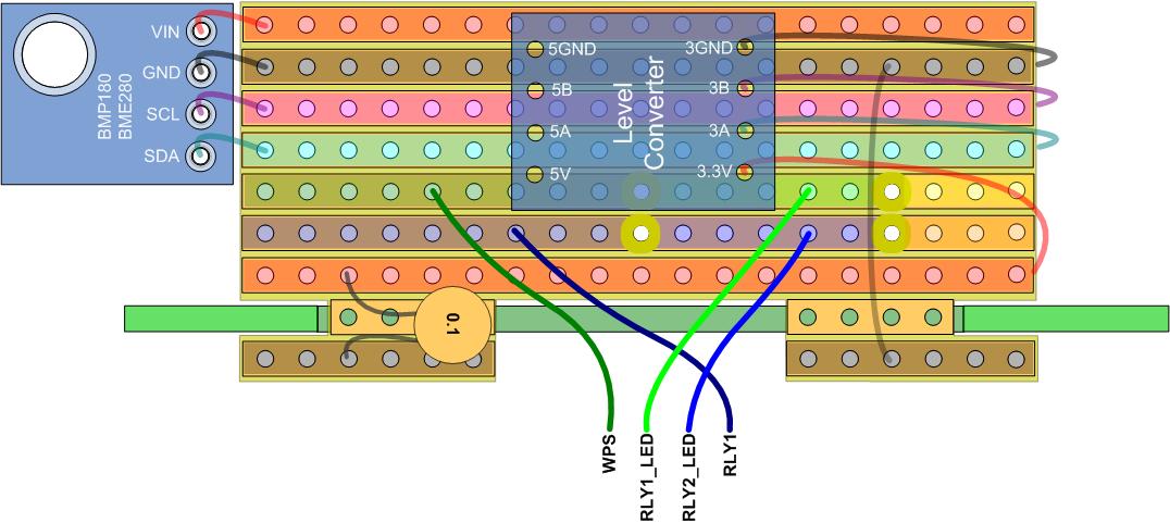
Route the wires up through the access slot and solder them directly to anywhere convenient along their appropriate copper tracks, as per the diagram above.
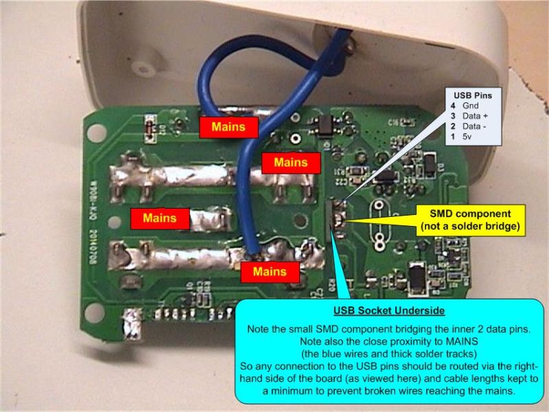
Remove the SMD component bridging the 2 inner USB socket pads on the underside of the Mains board, then solder 4 thin flexible wires to the USB pads. Route the wires towards the Button end of the Mains board (right-hand side of the picture) so that they go away from the Mains - then arc them back down and along the outer edge of the Mains board until they can be routed up through the access slot of the replacement wifi board.
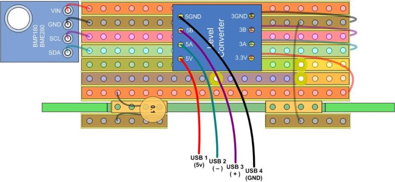
Trim the wires to fit into their appropriate Level Converter holes, then ease out the Level Converter module sufficient to solder the wires in place. Use a bit of double-sided tape afterwards to hold the module back where it belongs. Hold all the wires in place with some duct tape, and particularly the USB wires on the underside of the Mains board to prevent any possible broken wires from moving and touching any nasty Mains stuff.
Finally, stick duct tape over the wifi board to hold everything in place, then re-assemble.
###Flashing
Ensure the Smart Socket is not plugged into a Mains outlet… I cannot advocate flashing the Smart Socket while it is powered by Mains unless using non-contact OTA (Over The Air).
Make a simple USB Flashing Adapter by salvaging an old USB mouse cable with plug, then crimping on 4 female Duponts (or solder a bit of header socket) to the cut end for easy connection to the 5v UARTs appropriate pins, remembering to cross-connect RX and TX. Boot into flashing mode by holding down the on-board WPS button as the flashing adapter is plugged into the USB socket, then release the button and start the upload.
###External Sensors
I2c sensors such as the BME 280 sensor modules can offer things like barometric pressure, temp and humidity all on the same little i2c pcb, but you aren’t just limited to those.
A small PCF8591 AD/DA Converter Module (available for about £1) offers four i2c addressable analog channels, plus even includes on-board temp and LDR sensors.
A similarly addressable PCF8574 I/O expander can offer up to 8 digital channels (of mixed inputs/outputs) and an MCP23017 module offers 16 (both are cascadable for more).
If you want to use 3.3v sensors, include an AMS1117-3.3 module and level converter. Much flexibility is possible for various alternative plug-in digital and/or analog sensors, either plugged directly into the Smart Socket, or via USB extension cables and splitters.
So although originally only a hack ‘bonus’, the ability for plug-in external sensors actually offers a very useful and convenient mains-powered sensor platform just in its own right!
To see how useful, take a look at the ‘K2’ smart socket which has come on the market since I started this article (search AliExpress.com). It is probably unlikely to use an ESP8266 so therefore would probably need hacking to be Souliss compatable, but the important point to note is the fact that the manufacturer has standardised on a range of USB plug-in sensor modules, and that those neat USB plug-in sensors are sold separately.
They certainly give an idea of how useful the facility for external sensors could be, but perhaps they may also use i2c… in which case there could be a 50% chance of them being hardware compatable without even needing to swap the Smart Sockets 2 USB data wires.
Remember that i2c is a daisy-chained ‘bus’, so pullups are only needed on the last device in the chain - which means that some devices with onboard pullups (such as BMP180) may need their i2c pullups disabling (typically by removing a track link).
Adding or removing i2c devices is likely to affect the required value for the pullups, so if devices are expected to be changed, it may be better to use separate plug-in terminating resistor modules to allow quick changes of alternative value pullups when required.

You can get a handfull of these USB to DIP adapters for less than £2 from ebay. They can be soldered directly to your external sensor adapters, or use ‘flying’ wires for connecting to a small ‘development’ terminator breadboard offering quick-change i2c resistor selection, or they could directly accomodate the two i2c pullup resistors and then perhaps be neatly housed in any old unwanted USB dongles you might have lying around.
Those with an osilloscope could select for best resistor values by monitoring for the squarest i2c waveform, but others can use some lateral thinking to select for best communications speed and reliability (which is the real goal anyway). Loop commonly available i2c scanner code and keep checking for valid device responses as the i2c comms speed is progressively increased until the device response fails - now try substituting higher or lower value resistor pullup pairs (easy if using the above mentioned terminator breadboard) and keep repeating the speed test until unable to improve further… then you can more permanently install the ‘best’ i2c pullups with some confidence.
###Software
The Souliss ‘Smart Socket Hack’ example code gives ‘Basic’ wifi On/Off control of the relay, plus local manual On/Off toggle of the relay using the WPS button for test purposes. The simple ‘Basic’ Mains switching functionality could be usefully enhanced by software to offer additional benefits such as…
- Scheduled Control - automatic Daily/Weekly switching according to pre-set dates/times.
- Duration Timers - automatic switching Off or On after preset duration or delay.
- Reboot Sequence - SoulissApp Button to cause the selected device to power Off for 10 seconds then automatically back On again, for rebooting routers or servers etc (could also be auto-triggered by loss of connection if wished).
The inclusion of the internal temp sensor offers potential for a programmable thermostat.
Note: Electronics generates heat, therefore the temperature measured inside the Smart Socket (or any closed housing) is likely to be higher than the ambient temperature outside. To compensate for this, run the assembled Smart Socket long enough for the temperature readings to stabilise, then dismantle it and safely power it via USB to measure the ambient temperature and compare the difference after readings stabilise again. A simple software subtraction of that difference from the sensor reading in your program would then give the effective ambient temperature rather than the warmer level inside the Smart Socket.
OTA Web Configuration could allow all such Smart Socket features and sensors to be easily configured and enabled on an as needed basis, and hopefully that is just around the corner.
Alternatively, some simple i2c Scanner code could check responses of specific device addresses from a ‘possibles’ list to automatically discover and configure available sensors.
It is up to users to provide the software to suit their own needs and hardware options, and hopefully to contribute back their successes for the benefit of others.
###Footnotes
Although this hack was specifically developed for the Smart Socket, it is worth pointing out that all the features and expansion options are also equally as applicable for any home-built switched mains sockets… or any other devices it can be fitted into, for that matter.
A larger piece of stripboard could allow easier component placement and even accomodate an ESP-12 adapter plate if wished, plus offer room for things like side header pins for easy GPIO test access, flashing buttons, 3.3v regulator module and 470uF smoothing cap, etc.
The drawing above only suggests a possible starting point - your own stripboard shape and size should take advantage of available space to best accomodate your own required items.
For those wanting a more professional-looking result, a 5cm x 5cm ESP-12E printed circuit board offering similar functionality is available from Juan Pinto (link to go here). He can also supply populated boards if wished, including suitable Souliss software, plus a matching range of convenient 3D printed housings (including DIN Rail and Table Lamp versions).
And for those prefering the convenience of a completed and ready-to-use switched-mains socket, Lesjaw Ardi (link to go here) produces a range of ready-built Souliss items.
One of the problems when creating a home-built switched mains socket is how to power the electronics without using a second dedicated external mains plug just for powering the low voltage supply - which can makes things clunky, untidy, and unsatisfactory. Ideally the low voltage supply for the electronics would be included within the home-built switched socket housing, so here’s a cheap compact mains-derived PSU complete with USB charging socket that some people may not be aware of - it may not be the best option for everybody, but it is worth pointing out as a potential alternative that otherwise could be over-looked.
It’s available for just £1 and free postage off ebay, and in any colour you like - not that colour matters when the first thing to do is prise the plug apart to remove the 5V 1A USB charging module from within… and if it can be stuffed into a UK mains plug, it should be relatively easy to fit inside a home-built switched socket housing. (Anyone thinking ‘but I need a NON-UK version’ should be using battery power for their own safety!)
To find them, enable ‘Buy it now’, ‘Worldwide’ and ‘FreeP&P’ in the ebay side panel (do each separately and wait for the screen refresh between each option change), and similarly enter a ‘to’ price of £2 (or equivalent) to cut out the more expensive clutter - then do a search for ‘mains plug usb charger’, and find the cheapest resulting seller who delivers to your country.
You might want to do similar search options for ‘AMS1117-3.3 Module’, and perhaps again for ‘5v relay module 1 channel’, and also ‘Logic Level Converter’. All 4 items can be bought for a combined total of less than £4 including free delivery, and along with the Smart Socket hack could provide all the electronics needed to make a home-built switched mains socket… but I am only suggesting ingredients, what recipes you choose to cook up are down to you. Don’t forget you won’t have the Smart Sockets C11 capacitor to use as the smoothing cap for your 3.3v supply, so you will need to add one of your own - but you can salvage almost any low voltage electrolytic between 100uF and 1000uF (preferably mid value) for that job.
Another Smart Socket alternative worth considering is to put the ESP hack into an RF switched socket housing, or even a plug-in electronic timer (not a mechanical one) - they offer a safe and neat housing with integral mains plug and switched mains output socket, and are available much cheaper than the Smart Socket. You might even be able to retain use of the existing low voltage supply and/or the relay, but if you need to discard everything it could offer sufficient room to fit the replacement items, and perhaps even for a display.
Almost done, but this couldn’t be complete without giving special thanks to Dario for his brilliant concept and very thorough professional implementation of Souliss, and to Alessandro for his excellent and indispensable Souliss App, and to the many others who have contributed to making Souliss as good as it is, and thanks also to all of the Souliss community - and others - who take the time and effort to share their innovations for the benefit of us all.
And finally - this is my first real hack, my first tutorial, and my first experience of ESPs. So I am certainly no expert, nor the best person to be offering such advice - but rather than taking the quick easy selfish option of just implementing the hack for myself, I prefer taking the opportunity to offer a contribution for others to benefit from if they wish (and hopefully most can find something of interest from within, however small it may be). Discovering the Smart Socket circuitry was the easy part compared to evolving a suitable solution for diverse needs and skill levels, plus producing the subject matter for every picture, and creating every component used in the drawings from scratch and to scale. It’s been a large and lengthy task which has continually changed and grown, so please don’t expect everything to be set in stone and absolutely perfect, just consider it a collection of helpful tips for anyone who would welcome them until they are able to learn any better for themselves.